

The Elements of Innovation Discovered
The Elements of Innovation Discovered
Sorted by date Results 1 - 13 of 13
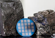
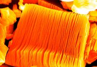
As the world continues to shift away from older technologies and carbon-emitting energy production, researchers have sought ways to reimagine their uses and align them with modern ideals. The number one candidate – coal – has been an energy lynchpin and an economic keystone for more than a century. Instead of cutting away the lifeline, science seeks to utilize this ancient material in new, high-tech ways. With companies turning coal into clean technologies such as bui...
Utilizing the bizarre capabilities of two-dimensional materials, researchers from the University of Minnesota, for the first time, have engineered an atomically thin material made from layers of molybdenum disulfide and graphene that can absorb nearly 100% light at room temperature, a discovery that could prove efficacious for a wide range of applications from optical communications to stealth technology. The scientists detailed their finding in "Achieving near-perfect light...

Liquid fuel rockets are adequate for jetting humans to the most popular destinations across our solar system in a reasonable amount of time – about three days to the Moon and six months to Mars. We, however, need a way of traveling near the speed of light to shave enough of the 75,000-year journey to get to Alpha Centauri, our closest solar system neighbor, in a human lifespan. This futuristic problem may be solved with one of humankind's earliest transportation t...
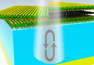
Developing on another element to the growing list of two-dimensional materials, researchers from the University of Twente in the Netherlands have demonstrated that germanene, a 2D material made of germanium atoms, can behave as a topological insulator – the first to consist of a single element – meaning it is comparable to transistors in that it can switch between on and off states for potentially more energy-efficient electronics. Topological insulators are materials wit...
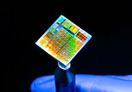
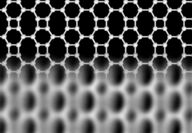
Marking the first of its kind and possibly the beginning of the next generation of computing, researchers from King Abdullah University of Science and Technology in Saudi Arabia have designed and demonstrated the world's first 2D microchip using synthetic materials. Since the first fabrication of atomically thin layers of graphite, graphene, in 2004, there has been intense interest in such materials for advanced and novel applications due to their exotic and promising...
An international team of researchers led by Drexel University has found that a thin coating of MXene could enhance a material's ability to trap or shed heat. The discovery, which is tied to the 2D material's ability to regulate the passage of ambient infrared radiation, could lead to advances in thermal clothing, heating elements, and new materials for radiative heating and cooling. "This research reveals yet another facet of MXene materials' versatility," said research lead...

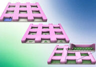
Researchers from the University of Chicago have discovered the secret recipe for creating MXene. Much like a croissant with its individual layers painstakingly kneaded twixt generous amounts of butter, this breakthrough results in a beautiful flakey 2D material that could usher in a new era of electronics. Until recently, MXenes (pronounced "max-eens") were as labor-intensive as good croissants in a French bakery. Involving several stringent chemical engineering steps,...
Struggling to overcome the inevitable shortcomings of miniaturizing digital technologies due to the inherent limits of silicon, Massachusetts Institute of Technology researchers have potentially reinstated Moore's Law with the synthesis of 2D materials on silicon wafers. True to Moore's Law, the number of transistors on a microchip has doubled every year since its origination in 1965; however, this trajectory is predicted to soon plateau because silicon – the backbone of m...

Much like lead can protect even Superman from the effects of kryptonite, researchers at Drexel University's College of Engineering may have engineered a vanadium-based MXene shield that could render electronic devices impermeable to electromagnetic waves, essentially protecting them from the multitude of frequencies whizzing about our heads every day. Buzzing, feedback or static are some of the most noticeable manifestations of electromagnetic interference. This is...
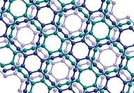
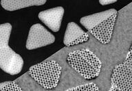
Though scientists have tried with limited success for more than a decade to synthesize a new form of carbon called "graphyne," a team of researchers at the University of Colorado Boulder has finally succeeded in creating the material in bulk. Graphyne has long interested the scientific community because of its similarities to graphene, another form of carbon highly valued by industry. Yet despite decades of work and theorizing, only a few fragments of graphyne have ever been...

In a discovery that could speed research into next-generation electronics and light-emitting diode devices, a University of Michigan research team has developed the first reliable, scalable method for growing single layers of hexagonal boron nitride (hBN) on graphene. Known as molecular-beam epitaxy – a process widely used in the manufacture of semiconductor devices, including transistors, and considered one of the fundamental tools for the development of nanotechnologies. Thi...
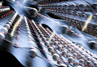
Roughly 200 times stronger than steel, highly conductive to electricity and heat, antibacterial, and only one atom thick, graphene is a wonder material that has captured the imagination of scientists. Now, researchers in Germany and Finland have created a new two-dimensional carbon material that offers new properties and possibilities. In recent years, graphene has been used to make materials lighter and stronger, batteries charge faster and last longer, and even as a coating...
An international team led by Massachusetts Institute of Technology researchers has discovered a method of imaging what goes on at the boundary of 2D and 3D materials, down to the level of individual atoms. In recent years, engineers have managed to develop ways to modify the properties of few "two-dimensional" materials – considered such by existing as a single atom in thickness. For practical applications however, two-dimensional materials like graphene and hexagonal boron n...