
The Elements of Innovation Discovered
The Elements of Innovation Discovered
Penn State discovery opens door to new classes of materials Metal Tech News – March 1, 2023
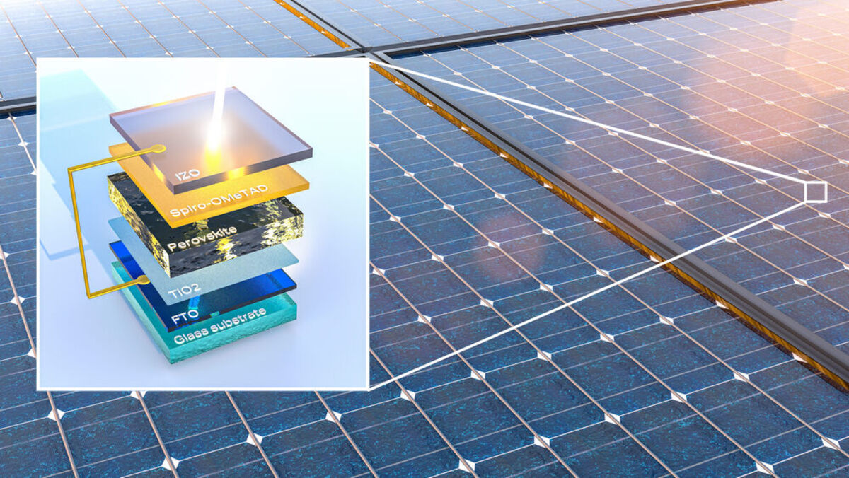
Separated into its constituent parts, this is an illustrated example of photovoltaic layers in a single, high-performance perovskite solar cell.
Over the last two decades, perovskite crystal lattices have been held as extremely promising materials in photovoltaic and light-emitting devices. This family of minerals exhibits unique electrical properties currently being utilized in solar cells.
A Penn State-led team has created a faster, more cost-effective process to fabricate larger perovskite devices than previously possible. Their reported findings were published in the journal Nature Communications and have opened a new field of inspiration for next-generation solar technology.
"This method we developed allows us to easily create very large bulk samples within several minutes, rather than days or weeks using traditional methods," says Luyao Zheng, lead author in the study and postdoctoral researcher in the Department of Materials Science at Penn State. "And our materials are high quality-their properties can compete with single-crystal perovskites."
The researchers use a method called spark plasma sintering, whereby a fine powder is heated by applying electric current and compressed into a solid or porous mass. This complete process is called electrical and mechanical field-assisted sintering technique (EM-FAST).
The results are 100% integration of the component raw ingredients into the final device, as opposed to only 20 to 30% in typical solution-based processing.
The mineral perovskite, named after the Russian mineralogist Count Lev Perovski, was first used in solar cells in 2009. While the number of natural perovskite minerals is limited, synthetic perovskites span the whole periodic table in terms of elemental composition, indicating that perovskite is a useful and highly adaptable type of crystal lattice to study.
The wet chemistry commonly used to create the perovskites used to manufacture solar cells liquifies raw materials in a potentially toxic solvent solution and then solidifies them into thin films. The approach is expensive and inefficient for larger applications.
A dry method developed by the Penn State team overcomes the shortcomings.
"Our technique is the best of both worlds," says Bed Poudel, Penn State professor and co-author of the study. "We get single-crystal-like properties, and we don't have to worry about size limitations or any contamination or yield of toxic materials."
Because the EM-FAST process uses dry materials, device components can be tailored to include further ingredients with properties that are otherwise incompatible with wet chemistry. This creates potential for producing layered compositions where manufacturers design specific devices that can be directly printed from dry powders.
"This opens up possibilities to design and develop new classes of materials, including better thermoelectric and solar materials, as well as X- and gamma-ray detectors," says Amin Nozariasbmarz, co-author and assistant research professor at Penn State. "Some of the applications are things we already know, but because this is a new technique to make new halide perovskite materials with controlled properties, structures, and compositions, maybe there is room in the future for new breakthroughs to come from that."
This is a step toward discovering additional perovskite compositions and uses, new materials compliant with the ongoing global demand for greener technologies, and the potential for cheaper carbon-neutral manufacturing technologies and higher throughput material synthesis.
"Because of the background we have, we were talking and thought we could change some parameters and try this with perovskites," Nozariasbmarz concludes. "And it just opened a door to a new world. This paper is a link to that door – to new materials and new properties."


Reader Comments(0)