
The Elements of Innovation Discovered
The Elements of Innovation Discovered
Finds specific temperature makes no folds, wrinkles, adlayers Metal Tech News – September 1, 2021
Imperfections in graphene result from baking at temperatures over 1,030 degrees Kelvin. At or below that temperature allows for near perfect sheets of the 2D wonder material.
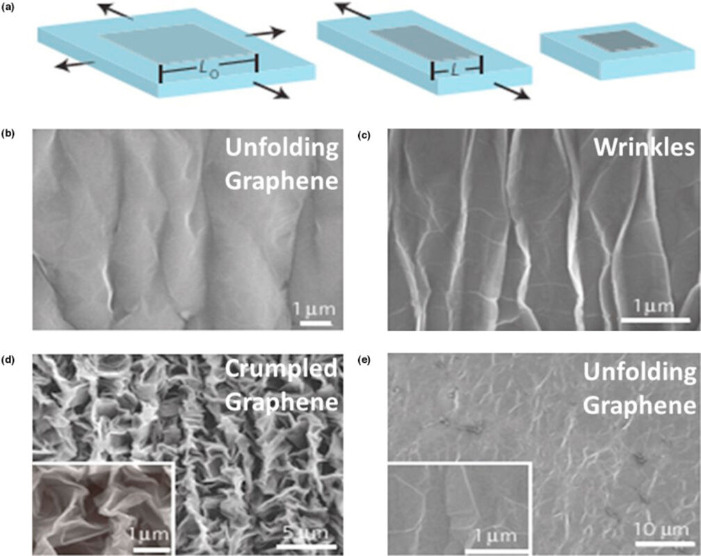
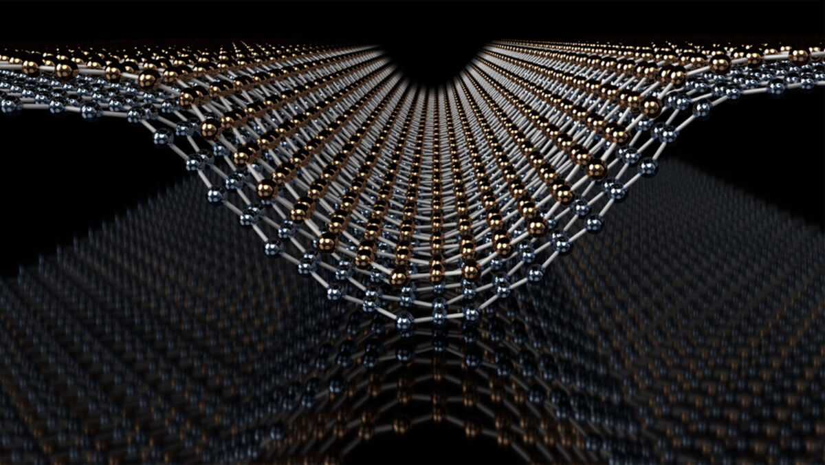
Much like a piece of paper that has been crumpled up, if you try to smooth it out, the wrinkles remain. Research into creating pristine, smooth graphene for better conductivity and other uses has been a goal for many scientists.
A team at the Center for Multidimensional Carbon Materials within the Institute for Basic Science in South Korea, including students at the Ulsan National Institute of Science and Technology, have achieved growth and characterization of large area, single-crystal graphene that has no wrinkles, folds or absorption layers. This could be said to be the most perfect graphene that has been grown and characterized, to date.
"This pioneering breakthrough was due to many contributing factors, including human ingenuity and the ability of CMCM researchers to reproducibly make large-area single-crystal copper-nickel foils, on which the graphene was grown by chemical vapor deposition using a mixture of ethylene with hydrogen in a stream of argon gas," said Rod Rouff, director at the Center for Multidimensional Carbon Materials.
The research team had previously reported single-crystal and absorption layer-free or adlayer-free films of graphene grown using methane at temperatures of approximately 1,320 degrees Kelvin on copper foils.
However, these films always contained long folds that are the consequence of tall wrinkles that form as the graphene is cooled from the growth temperature down to room temperature. Furthermore, the folds would also contain cracks that ultimately lower the mechanical strength of the graphene.
To overcome this drawback, CMCM researchers devised a series of experiments that involved "cycling" the temperature immediately after growing the graphene at 1,320 K. This resulted in learning that the folds are formed at or above 1,020 K during the cooling process.
After learning this, the team decided to grow graphene on copper-nickel foils at several different temperatures, which led to the discovery that large-area, high-quality, fold-free, and adlayer-free single-crystal graphene films could be grown in a temperature range of between 1,000 K and 1,030 K.
Possibly even more important, the research team was able to scale up the graphene production using this method, as it was successfully grown on five foils – at dimensions no larger than four by seven centimeters (1.6 by 2.8 inches) – simultaneously in a 15.2-cm (six inches) diameter home-built quartz furnace.
"Our method of growing fold-free graphene films is very reproducible, with each foil yielding two identical pieces of high-quality graphene films on both sides of the foil," said Meihui Wang, a student in the research group. "By using the electrochemical bubbling transfer method, graphene can be delaminated in about one minute and the copper-nickel foil can be quickly readied for the next growth-transfer cycle."
In the process of achieving fold-free single-crystal graphene, the researchers also discovered the reasons behind the formation of these folds in the first place.
High-resolution transmission electron microscopy imaging was performed to observe the cross-sections of the samples grown above 1,040 K and so was discovered that the deadhesion – a detachment of a cell from a surface to which it was once adhering – was the cause. This happens at "bunched step edge" regions between the single crystal copper-nickel plateaus.
"We discovered that step-bunching of a copper-nickel foil surface suddenly occurs at about 1030 K, and this 'surface reconstruction' is the reason why the critical growth temperature of fold-free graphene is at approximately 1,030 K or below," added Ruoff.
The advent of such large-area, fold-free, single-crystal graphene film could allow for the straightforward fabrication of integrated high-performance devices oriented in any direction over the entirety of the film.
These films will be important for further advances in basic science, which may lead to new applications in electronic, photonic, mechanical, thermal and other such areas. The near-perfect graphene is also useful for stacking, either with itself or with other 2D materials, which could further expand the range of likely applications.
Given that the copper-nickel foils can be used repeatedly and that the graphene can be transferred to other substrates in less than a minute, the scalable manufacturing of this process is possibly the most significant discovery of all.


Reader Comments(0)