
The Elements of Innovation Discovered
The Elements of Innovation Discovered
MIT researchers solve problem stagnating next-gen processors Metal Tech News - January 25, 2023
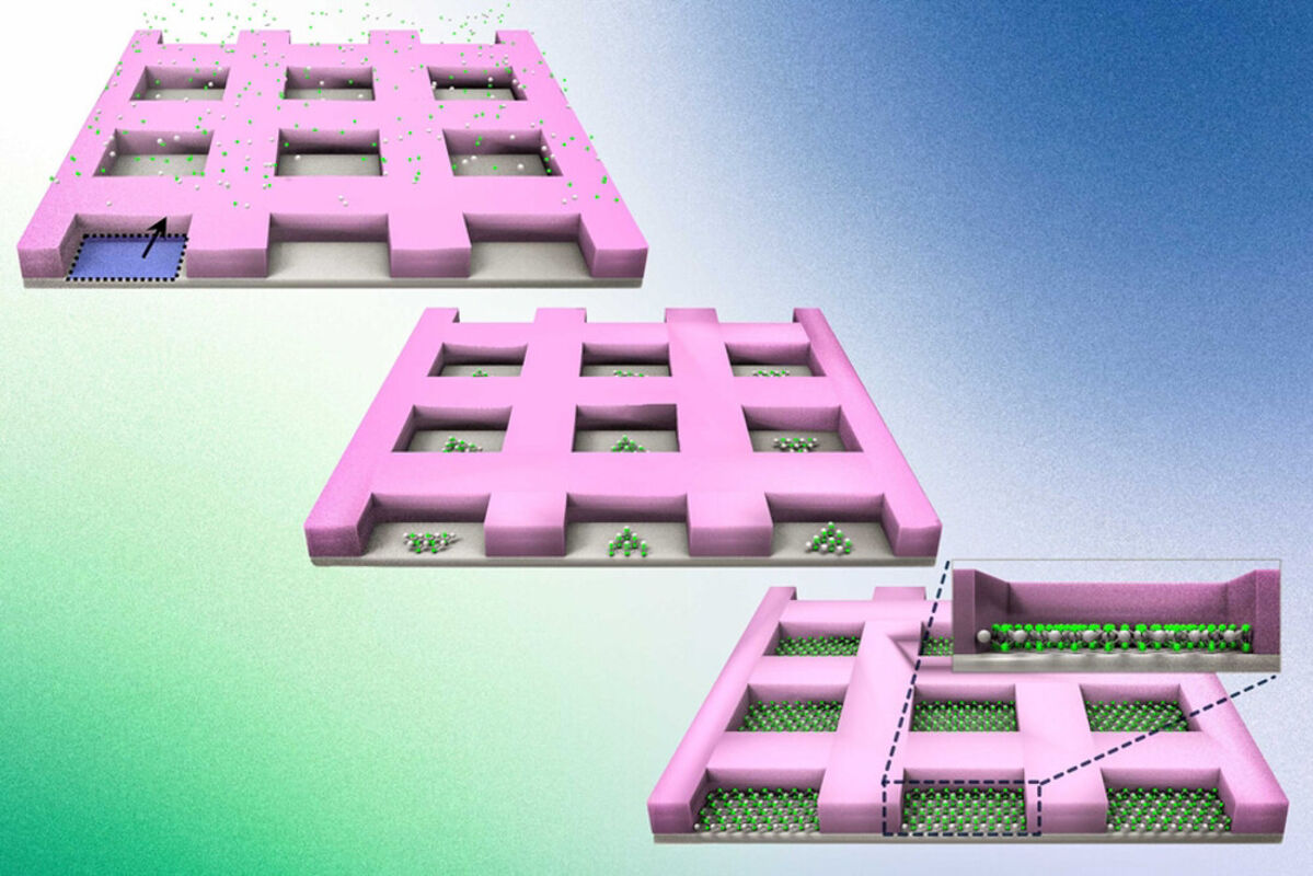
By depositing atoms on a wafer coated in a "mask" (top left), MIT engineers can corral the atoms in the mask's individual pockets (center middle), and encourage the atoms to grow into perfect, 2D, single-crystalline layers (bottom right).
Struggling to overcome the inevitable shortcomings of miniaturizing digital technologies due to the inherent limits of silicon, Massachusetts Institute of Technology researchers have potentially reinstated Moore's Law with the synthesis of 2D materials on silicon wafers.
True to Moore's Law, the number of transistors on a microchip has doubled every year since its origination in 1965; however, this trajectory is predicted to soon plateau because silicon – the backbone of modern transistors – loses the electrical properties that have enabled technology to reach its present-day feats when this material is used below certain sizes.
Enter 2D materials – sheets of perfect crystalline structures that are as thin as a single atom. At the scale of nanometers, 2D materials can conduct electrons far more efficiently than silicon; hence the search for next-generation transistor materials has focused on 2D materials as potential successors to silicon.
Before electronics can even begin to use 2D materials, however, scientists must first find a way to engineer the materials on industry-standard silicon wafers while preserving their perfect crystal form. And MIT engineers may now have a solution.
Developing a method that could enable chip manufacturers to fabricate ever-smaller transistors from 2D materials, this new method is a form of "nonepitaxial, single-crystalline growth," which the team used for the first time to grow pure, defect-free 2D materials onto industrial silicon wafers.
With this method, the team then fabricated a simple, functional transistor from a type of 2D material called transition-metal dichalcogenides, or TMDs, which are known to conduct electricity better than silicon at the nanoscale.
"We expect our technology could enable the development of 2D semiconductor-based, high-performance, next-generation electronic devices," said Kim Jeehwan, associate professor of mechanical engineering at MIT. "We've unlocked a way to catch up to Moore's Law using 2D materials."
To produce a 2D material, researchers have typically employed a manual process by which an atom-thin flake is carefully exfoliated from bulk material, like peeling away the layers of an onion.
But most bulk materials are polycrystalline or contain multiple crystals that grow in random orientations.
Where one crystal meets another, the "grain boundary" acts as an electric barrier. Any electrons flowing through one crystal suddenly stop when met with a crystal of a different orientation, damping a material's conductivity.
Even after exfoliating a 2D flake, researchers must then search for the flake for "single-crystalline" regions – a tedious and time-intensive process that is difficult to execute at industrial scales.
Recently, researchers have found other ways to fabricate 2D materials by growing them on wafers of sapphire – a material with a hexagonal pattern of atoms that encourages 2D materials to mimic the same structure.
"But nobody uses sapphire in the memory or logic industry," said Jeehwan. "All the infrastructure is based on silicon. For semiconductor processing, you need to use silicon wafers."
Nevertheless, wafers of silicon lack sapphire's hexagonal supporting scaffold. When researchers attempt to grow 2D materials on silicon, the result is a random patchwork of crystals that merge haphazardly, forming numerous grain boundaries that stymie conductivity.
"It's considered almost impossible to grow single-crystalline 2D materials on silicon," Jeehwan continued. "Now we show you can. And our trick is to prevent the formation of grain boundaries."
The team's new nonepitaxial, single-crystalline growth does not require peeling and searching for flakes in a haystack. Instead, the researchers use conventional vapor deposition methods to pump atoms across the wafer.
Eventually settling on the wafer through condensation, these atoms grow into two-dimensional crystal orientations. If left alone, each "nucleus," or seed of a crystal, would grow in random orientations across the silicon wafer.
But Jeehwan and colleagues found a way to align each growing crystal to create single-crystalline regions across the entire wafer.
To do so, they first covered a silicon wafer in a "mask" – a coating of silicon dioxide that they then patterned into a tiny pocket, each designed to trap a crystal seed. Across the masked wafer, they then flowed a gas of atoms that settled into each pocket to form a 2D material – in this case, a TMD.
The mask's pockets corralled the atoms and encouraged them to assemble on the silicon wafer in the same single-crystalline orientation.
"That is a very shocking result," the MIT researcher said. "You have single-crystalline growth everywhere, even if there is no epitaxial relation between the 2D material and silicon wafer."
With their masking method, the team was able to fabricate a simple TMD transistor and showed that its electrical performance was just as good as a pure flake of the same material.
"Until now, there has been no way of making 2D materials in single-crystalline form on silicon wafers, thus the whole community has been struggling to realize next-generation processors without transferring 2D materials," said Jeehwan. "Now we have completely solved this problem, with a way to make devices smaller than a few nanometers. This will change the paradigm of Moore's Law."


Reader Comments(0)