The Elements of Innovation Discovered

Diamonds can act like metals in devices

Researchers use strain to transform diamonds into conductors Metal Tech News – October 28, 2020
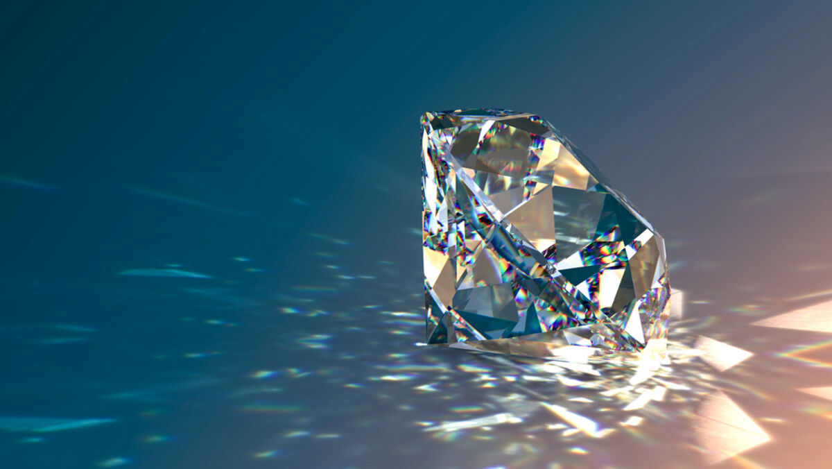
Diamonds are well known as the hardest minerals on earth. The sparkling gemstones also are exceptional thermal conductors and electrical insulators.

Now, an international team of researchers says diamonds have yet another distinction – they can exhibit the properties of metals.

The discovery, first reported Oct. 5 in the "Proceedings of the National Academy of Sciences," could write a new chapter in the saga of diamonds used in sophisticated technological and industrial applications.

The technical paper describes the work of Professor Ju Li and graduate student Zhe Shi of Massachusetts Institute of Technology; Principal Research Scientist Ming Dao; Professor Subra Suresh, who is president of Nanyang Technological University in Singapore as well as a former dean of engineering; and MIT Professor Emeritus Vannevar Bush; and Evgenii Tsymbalov and Alexander Shapeev at the Skolkovo Institute of Science and Technology in Moscow.

The research also was supported by the U.S. Office of Naval Research.

The researchers discovered a way to tweak tiny needles of diamond in a controlled manner to transform their electronic properties, dialing them from insulating, through semiconducting, to highly conductive, or metallic. They also found that the process can be induced dynamically and reversed at will, with no degradation of the diamonds.

Using a combination of quantum mechanical calculations, analyses of mechanical deformation, and machine learning, the team demonstrated that the phenomenon, long-theorized as a possibility, really can occur in nanosized diamonds.

Variety of applications

Though still at an early proof-of-concept stage, the discovery may open up a wide array of potential applications, including new kinds of broadband solar cells, highly efficient LEDs and power electronics, and new optical devices or quantum sensors, the researchers say.

The concept of straining a semiconductor material such as silicon to improve its performance found applications in the microelectronics industry more than 20 years ago. However, that approach entailed small strains on the order of about 1%.

Li and his collaborators have spent years developing the concept of "elastic strain engineering." This is based on the ability to cause significant changes in the electrical, optical, thermal, and other properties of materials simply by deforming them, or putting them under moderate to large mechanical strain, enough to alter the geometric arrangement of atoms in the material's crystal lattice but without disrupting that lattice.

Strain engineering breakthrough

In a major advance in 2018, a team led by Suresh, Dao, and Yang Lu from the City University of Hong Kong showed that tiny needles of a diamond, just a few hundred nanometers across, could be bent without fracture at room temperature to large strains. They were able to repeatedly bend these nanoneedles to tensile strain as much as 10%; the needles can then return intact to their original shape.

The key to this work is a property known as "bandgap," which essentially determines how readily electrons can move through a material. This property is thus key to the material's electrical conductivity. Diamonds normally have a very wide bandgap of 5.6 electron volts, meaning they are strong electrical insulators that electrons do not move through readily. In their latest simulations, the researchers show that a diamond's bandgap can be gradually, continuously, and reversibly changed, providing a wide range of electrical properties, from insulator through semiconductor to metal.

"We found that it's possible to reduce the bandgap from 5.6 electron volts ... to zero," Li said. "The point of this is that if you can change continuously from 5.6 to 0 electron volts, then you cover all the range of bandgaps. Through strain engineering, you can make a diamond have the bandgap of silicon, which is most widely used as a semiconductor, or gallium nitride, which is used for LEDs. You can even have it become an infrared detector or detect a whole range of light ... from the infrared to the ultraviolet part of the spectrum."

Many applications

"The ability to engineer and design electrical conductivity in a diamond without changing its chemical composition and stability offers unprecedented flexibility to custom-design its functions," said Suresh. "The methods demonstrated in this work could be applied to a broad range of other semiconductor materials of technological interest in mechanical, microelectronics, biomedical, energy and photonics applications, through strain engineering."

A single tiny piece of diamond, for example, can be bent so a solar cell is capable of capturing all frequencies of light on a single device, something that currently can only be achieved through tandem devices that couple different kinds of solar cell materials together in layers to combine their different absorption bands. These might someday be used as broad-spectrum photodetectors for industrial or scientific applications.

One constraint, which required not only the right amount of strain but also the right orientation of the diamond's crystalline lattice, was to prevent the strain from causing the atomic configuration to cross a tipping point and turning into graphite, the soft material used in pencils, the researchers noted.

The process also can transform a diamond into two types of semiconductors, either "direct" or "indirect" bandgap semiconductors, depending on the intended application. For solar cells, for example, direct bandgaps provide a much more efficient collection of energy from light, allowing them to be much thinner than materials such as silicon, which has an indirect bandgap that requires a much longer pathway to collect a photon's energy.

Li suggested that the new process could be relevant for a wide variety of potential applications, such as highly sensitive quantum-based detectors that use defects and dopant atoms in a diamond.

"Using strain, we can control the emission and absorption levels of these point defects," allowing novel ways of controlling their electronic and nuclear quantum states, he explained.

A wide variety of conditions are made possible by the different dimensions of strain variations. This means, "if we have a particular application in mind, then we could optimize toward that application target," Li observed. "And what is nice about the elastic straining approach is that it is dynamic," so that it can be continuously varied in real-time, as needed.

The early-stage proof-of-concept work is not yet at the point where practical devices can be designed. But with the ongoing research, the researchers said they expect practical applications could be possible, partly because of promising work being done around the world on the growth of homogenous diamond materials, or diamonds comprised of uniformly distributed particles.


Reader Comments(0)