The Elements of Innovation Discovered

Scientists explore new atomic frontiers

Studying atom-thick layers of MXenes leads to new discoveries Metal Tech News – October 5, 2022
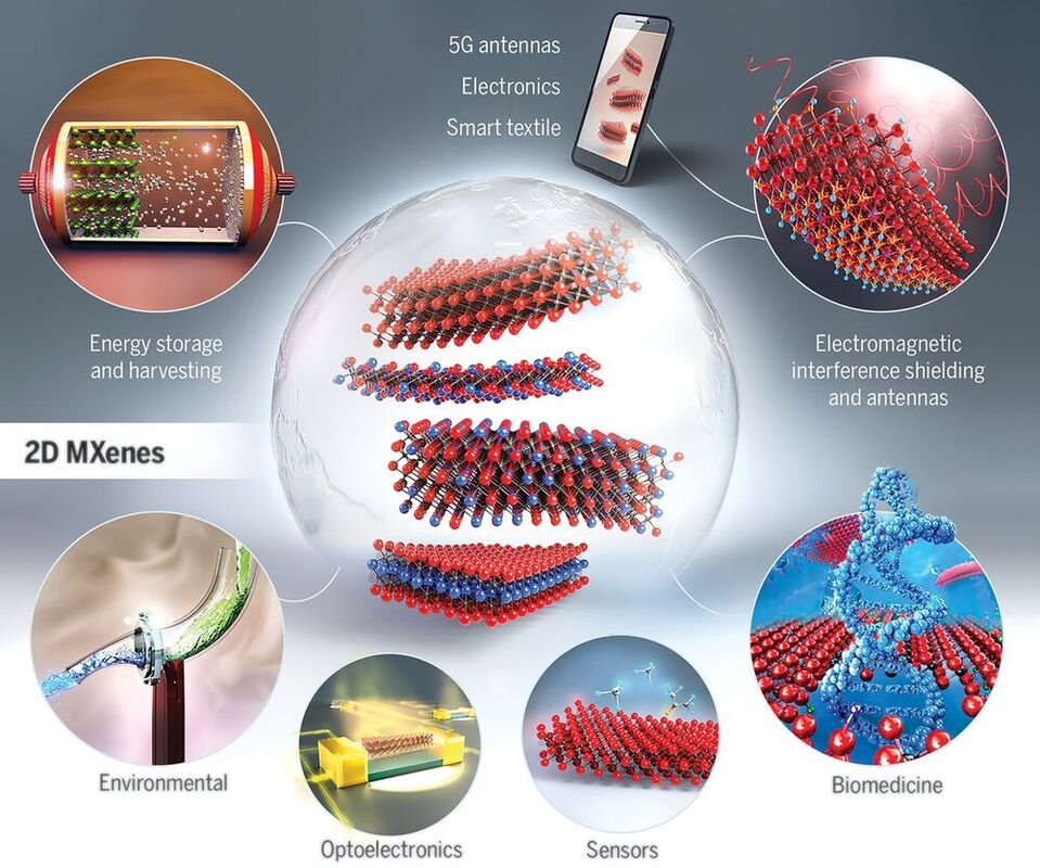
Researchers at Drexel University in Philadelphia have succeeded in using a new method of analysis to peel back the atomic layers of two-dimensional metallic compounds known as MXenes (pronounced max-eens), opening the door to development of a wide range of new materials.

Two-dimensional materials are substances with a thickness of a few nanometers or less. Electrons in these materials are free to move in the two-dimensional plane, but their restricted motion in the third direction is governed by quantum mechanics. Prominent examples include quantum wells and graphene.

MXenes, 2D ceramics made from bulk crystals called MAX, have shown promise for use in energy storage applications such as lithium-ion batteries and supercapacitors, as well as for photocatalysts, water purifiers, gas sensors, transparent conducting electrodes, neural electrodes and other energy storage devices.

Since the initial discovery of MXenes in 2011, Drexel University researchers have made steady progress in understanding the physical and electrochemical properties and complex chemical composition and structure of this rapidly growing family of exceptionally versatile materials.

More than a decade later, advanced instruments and a new approach have allowed the Drexel scientists to peer within the atomic layers to better understand the connection between the materials' form and function.

Discovery unlocks potential

In a paper published Sept. 22 in Nature Nanotechnology, researchers from Drexel's College of Engineering and Poland's Warsaw Institute of Technology and Institute of Microelectronics and Photonics reported a new way to look at the nanomaterials by observing atoms that make up MXenes and their precursor materials, MAX phases, using a technique called "secondary ion mass spectrometry."

The report is titled "Oxycarbide MXenes and MAX phases identification using monoatomic layer-by-layer analysis with ultralow-energy secondary-ion mass spectrometry."

The Drexel-led group discovered atoms in unexpected locations and imperfections in 2D materials that could explain some of their unique physical properties. They also demonstrated the existence of a new subfamily of MXenes, called oxycarbides, which are two-dimensional materials where up to 30% of carbon atoms are replaced by oxygen.

This discovery will enable scientists to build new MXenes and other nanomaterials with tunable properties best suited for specific applications, including antennas for 5G and 6G wireless communication, shields for electromagnetic interference, filters for hydrogen production, storage and separation, and wearable kidneys for dialysis patients.

"Better understanding of the detailed structure and composition of two-dimensional materials will allow us to unlock their full potential," said Yury Gogotsi, Ph. D., Distinguished University and Bach professor in Drexel's College of Engineering, who led the MXene characterization research.

"We now have a clearer picture of why MXenes behave the way they do and will be able to tailor their structure and therefore behaviors for important new applications," Gogotsi said.

Sputtering atom-thick layers

Secondary ion mass spectrometry, or SIMS, is a commonly used technique to study solid surfaces and thin films and how their chemistry changes with depth. It works by shooting a beam of charged particles at a sample, which bombards the atoms on the surface of the material and ejects them – a process called "sputtering."

The ejected ions are detected, collected, and identified based on their mass and serve as indicators of the composition of the material.

While SIMS has been used to study multi-layered materials over the years, the depth resolution of the technique has been limited to examining the surface of a material (several angstroms deep).

An angstrom is equal to one hundred millionth of a centimeter and is used mainly to express wavelengths and interatomic distances.

A team led by Pawel Michalowski, Ph. D., at Poland's Institute of Microelectronics and Photonics made a number of improvements to the technique, including adjusting the angle and energy of the beam and how the ejected ions are measured as well as cleaning the surface of the samples. This allowed researchers to sputter samples layer by layer to view with an atom-level resolution that had not been previously possible.

"The closest technique for analysis of thin layers and surfaces of MXenes is X-ray photoelectron spectroscopy, which we have been using at Drexel starting from the discovery of the first MXene," said Mark Anayee, a doctoral candidate in Gogotsi's group. "While XPS only gave us a look at the surface of the materials, SIMS lets us analyze the layers beneath the surface. It allows us to 'remove' precisely one layer of atoms at a time without disturbing the ones beneath it. This can give us a much clearer picture that would not be possible with any other laboratory technique."

Pathbreaking discoveries

As the team peeled back the upper layer of atoms, they began to see the subtle features of the chemical scaffolding within the layers of materials, revealing the unexpected presence and positioning of atoms and various defects and imperfections.

"We demonstrated the formation of oxygen-containing MXenes, so-called oxycarbides. This represents a new subfamily of MXenes – which is a big discovery!" said Gogotsi. "Our results suggest that for every carbide MXene, there is an oxycarbide MXene, where oxygen replaces some carbon atoms in the lattice structure."

Since MAX and MXenes represent a large family of materials, the researchers further explored more complex systems that include multiple metal elements. They made several pathbreaking observations, including the intermixing of atoms in chromium-titanium carbide MXene – which were previously thought to be separated into distinct layers. And they confirmed previous findings, such as the complete separation of molybdenum atoms to outer layers and titanium atoms to the inner layer in molybdenum-titanium carbide.

These findings are important for developing MXenes with a finely tuned structure and improved properties, according to Gogotsi.

"We can now control not only the total elemental composition of MXenes, but also know in which atomic layers the specific elements like carbon, oxygen, or metals are located," he said. "We know that eliminating oxygen helps to increase the environmental stability of titanium carbide MXene and increase its electronic conductivity. Now that we have a better understanding of how much additional oxygen is in the materials, we can adjust the recipe – so to speak – to produce MXenes that do not have it, and as a result, (are) more stable in the environment."

The Drexel team also plans to explore ways to separate layers of chromium and titanium, which will help to develop MXenes with attractive magnetic properties.

Mapping uncharted territory

Now that the SIMS technique has proven to be effective, Gogotsi plans to use it in future research, including his recent $3 million U.S. Department of Energy-funded effort to explore MXenes for hydrogen storage – an important step toward the development of a new sustainable energy source, he said.

"In many ways, studying MXenes for the last decade has been mapping uncharted territory," said Gogotsi. "With this new approach, we have better guidance on where to look for new materials and applications."

Co-authors of the paper include Sylwia Kozdram Iwona, Jóźwik, Anna Piatkowska, Mołgorzata Możdżonek, Agnieszka Malinowska, Ryszard Diduszko, and Edyta Wierzbicka, from the Institute of Microelectronics and Photonics; and Tyler S. Mathis and Kanit Hantanasirisakul, from Drexel; and Adrianna Wójcik from both the Institute of Microelectronics and Warsaw Institute of Technology.

The work was funded by Poland's National Science Centre and National Centre for Research and Development, the U.S. Department of Energy and the National Science Foundation.


Reader Comments(0)