
The Elements of Innovation Discovered
The Elements of Innovation Discovered
KAUST scientists successfully make with synthetic materials Metal Tech News – June 7, 2023
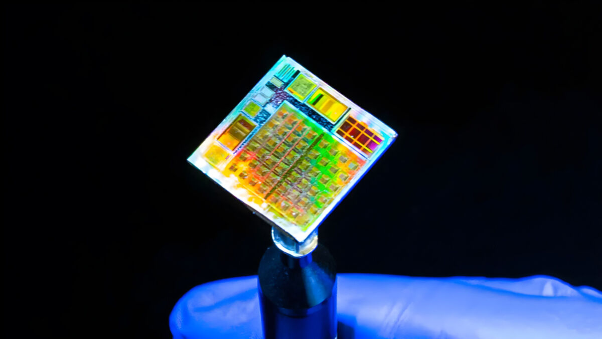
A King Abdullah University of Science and Technology research team has created a functioning microchip with 2D materials.
Marking the first of its kind and possibly the beginning of the next generation of computing, researchers from King Abdullah University of Science and Technology in Saudi Arabia have designed and demonstrated the world's first 2D microchip using synthetic materials.
Since the first fabrication of atomically thin layers of graphite, graphene, in 2004, there has been intense interest in such materials for advanced and novel applications due to their exotic and promising physical properties.
Despite decades of research, however, functional microdevices based on 2D materials have proved elusive due to the challenges in fabricating and handling such fragile thin films.
Inspired by recent 2D film breakthroughs out of the lab of KAUST Associate Professor Mario Lanza, the university research team has now produced and demonstrated a prototype 2D-based microchip.
"Our motivation was to increase the technology readiness level of 2D material-based electronic devices and circuits by using conventional silicon-based CMOS (complementary metal oxide semiconductor) microcircuits as a base and standard semiconductor fabrication techniques," said Lanza. "The challenge, however, is that synthetic 2D materials can contain local defects such as atomic impurities that can cause small devices to fail. Also, it is very difficult to integrate the 2D material into the microchip without damaging it."
To overcome these challenges, the fabrication of the 2D material takes precedence. Thus, the research team first optimized the design of the chip to make it easier to fabricate and minimize the effect of defects.
They did this by fabricating standard CMOS transistors on one side of the chip and feeding interconnects through to the underside, where the 2D material could be transferred reliably in small sections less than 0.25 micrometers or 0.00025 millimeters across.
"We produced the 2D material – hexagonal boron nitride, or h-BN, on copper foil – and transferred it to the microchip using a low-temperature wet process, and we then formed electrodes over the top by conventional vacuum evaporation and photolithography, which are processes we have in-house," said Lanza. "In this way we produced a five-by-five arrow of one-transistor/one-memristor (memory resistors) cells connected in a crossbar matrix."
The exotic properties of 2D h-HB make it an ideal "memristor" – a resistive component whose resistance can be set by applied voltage and remembers to switch on and off depending on that voltage.
In the five-by-five arrangement, each of the microscale memristors pads is connected to a single dedicated transistor. This provides the fine voltage control needed to operate the memristor as a functional device with high performance and reliability over thousands of cycles, in this case, as a low-power neural network element.
"With this flagship breakthrough, we are now talking with leading semiconducting companies to keep working in this direction," the KAUST professor said. "We are also considering installing our own wafer-scale industrial processing system for 2D materials at KAUST to advance this capability."


Reader Comments(0)