The Elements of Innovation Discovered

Quantum dot transistor gets green light

Copper-indium-selenide overcomes heavy metal limitations Metal Tech News – Nov. 11, 2020
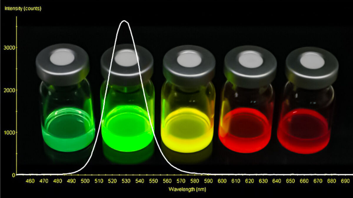
A recent scientific breakthrough in the metals used for transistors may change the face of all conventional electronics, providing new circuitry and electronics with the simply named quantum dot.

Researchers at Los Alamos National Laboratory in collaboration with the University of California, Irvine have managed to create functional logic circuits with the electronic building blocks known as quantum dots.

This innovation could promise a cheaper and production-friendly approach to complex electronic devices by simply fabricating in a chemistry lab, solution-based techniques to develop in demand components for a host of devices.

The team have been successful in demonstrating an integration of both positive and negative semiconductors in a single layer by using copper-indium-selenide quantum dots, which overcomes the heavy metal toxicity hurdle of lead and cadmium that limited previous advancements in nanocrystal technology.

The discovery of this new non-toxic material for quantum dots is attractive in realizing new types of flexible electronic circuits that could theoretically be printed onto virtually any surface, including plastic, paper and even human skin.

"Potential applications of the new approach to electronic devices based on non-toxic quantum dots include printable circuits, flexible displays, lab-on-a-chip diagnostics, wearable devices, medical testing, smart implants, and biometrics," said Victor Klimov, a physicist specializing in semiconductor nanocrystals at Los Alamos and lead author on the paper announcing the new results in the October 19 issue of Nature Communications.

The innovation that Klimov and colleagues have presented in their paper have defined positive and negative type transistors by applying two different types of metal contacts, gold and indium, respectively.

As further proof of practical utility of the developed approach, they were able to create functional circuits that performed logical operations.

With these quantum dots, being sized in the nanometers, the capabilities of smaller, smarter, more powerful and efficient circuitry could lead to innovations only before known of in science fiction.

Quantum dots

For decades, microelectronics has relied on extra-high purity silicon processed in special clean-room environments.

However, this is being challenged by several alternative technologies that allow for fabricating complex electronic circuits outside a clean room, via inexpensive, readily accessible chemical techniques.

Semiconductor nanoparticles made with chemistry methods is one such emerging technology, and due to their small size and unique properties directly controlled by quantum mechanics, these particles have been dubbed quantum dots.

While the first quantum dot transistors have been demonstrated for nearly 40 years, getting around the inherent nature of negative and positive electrical charges on a single layer proved a long-standing challenge.

Additionally, most efforts to bypass this restriction utilizing quantum dot transistors focused on nanocrystals based on lead and cadmium, highly toxic metals which greatly limited practical use.

A quantum dot consists of a semiconductor core covered with organic molecules.

As a result of this hybrid nature, they combine the advantages of well-understood traditional semiconductors with the chemical versatility of molecular systems.

Simply put, quantum dots are man-made nanoscale crystals that can transport electrons.

Largely a central topic in nanotechnology, when quantum dots are illuminated by ultraviolet light, the electron within the dot becomes excited to a state of higher energy, this means specific dot crystal sizes change the light emitted when hit by UV.

As energy is related to wavelength (color), this means that the optical properties of the particle can be finely tuned depending on its size.

Thus, particles can be made to emit or absorb specific colors, merely by controlling their size.

With this shift of energy, the change in the circuit can be used to quantify either an on or an off, a transistor at the nanometer scale.

For example, blue light can be let through a nanocrystal measuring roughly 450 nanometers small.

To provide a better sense of the potential of these transistors, the average human hair is about 75,000 nanometers thick. So, 167 of these nanocrystals lined up side-by-side would be about the width of a single hair strand.

The capability of possibly soon having nanotechnology transistors easily at the ready, without the manufacturing drawbacks of rigid and comparably huge silicon chips, will likely usher in a new era of flexible tech.

And the quantum dots materials breakthrough made by researchers at Los Alamos National Labs may very well be the catalyst for a chain reaction that changes all future technology as we know it.


Reader Comments(0)