
The Elements of Innovation Discovered
The Elements of Innovation Discovered
MIT discovers method to image interface between 2D and 3D Metal Tech News – March 3, 2021
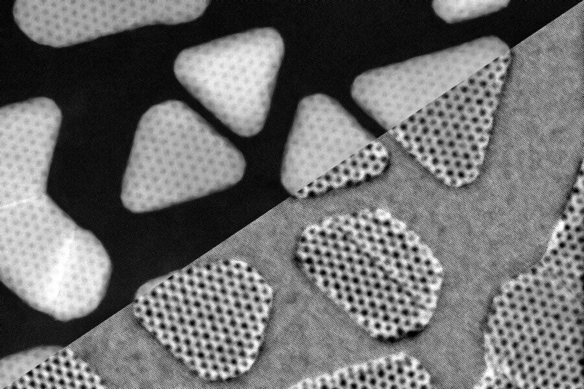
The imaged "island" of gold atoms, deposited on a layer of two-dimensional molybdenum sulfide, was produced by two different modes of the scanning tunneling electron microscope (STEM) in the new MIT.nano facility.
An international team led by Massachusetts Institute of Technology researchers has discovered a method of imaging what goes on at the boundary of 2D and 3D materials, down to the level of individual atoms.
In recent years, engineers have managed to develop ways to modify the properties of few "two-dimensional" materials – considered such by existing as a single atom in thickness.
For practical applications however, two-dimensional materials like graphene and hexagonal boron nitride must, at some point, connect with the ordinary world of 3D materials.
The team at MIT was able to discover a method of imaging what goes on at the intersection points, using advanced electron microscopes, where these materials meet between the two-dimensional and into the third.
By stacking two layers together and offsetting one of them, something known as moiré patterns are created, and these tiny shifts in alignment of atoms between two layers create a larger-scale pattern. It just so happens, that this also changes the way electrons move through the material, and in potentially useful ways.
Pairs of 2D materials, such as graphene or hexagonal boron nitride can exhibit incredible variations in behavior when two sheets are laid askew.
While these pairings have attracted scientific attention worldwide, little has been known about what happens when 2D materials meet regular 3D solids.
"What got us interested in this topic," said Francis Ross, professor of materials science and engineering at MIT. "What happens when a 2-D material and a 3-D material are put together. Firstly, how do you measure the atomic positions at, and near, the interface? Secondly, what are the differences between a 3D-2D and a 2D-2D interface? And thirdly, how you might control it –is there a way to deliberately design the interfacial structure (to produce the desired properties)?"
Finding out exactly what is taking place at such 2D-3D interfaces was a difficult challenge because the electron microscopes used to image this interaction was limited due to the very nature of 2D materials, which greatly inhibited the team's ability to extract depth information needed to analyze details of the structure.
However, the team determined a set of algorithms that allowed them to extrapolate back from the images of the sample, which looked somewhat like a set of overlapping shadows.
Unlike stacked 2D materials to create moiré patterns – picking up one layer, shifting it slightly and placing it back down again – the bonds holding 3D materials together are much stronger, so the team had to develop a new way of obtaining aligned layers for solids.
Adding a 3D material onto the 2D material in an ultrahigh vacuum, they were basically able to "grow" the arrangement of molecules, where the layers self-assembled in a reproducible orientation with specific degrees of twist.
After this, they had to figure out how to reveal the atomic configurations and orientations of the different layers, which involved state-of-the-art scanning transmission electron microscopes (STEM) found at MIT.nano, which generated a probe of electrons that are unusually narrow and precise and was able to scan the atomic structure.
Using even further complex techniques – called 4-D STEM – the research team was finally able to extract the full structure of the interface in the image.
"Now that we can image the full structure at the interface," said Georgios Varnavides, an MIT graduate student. "What does this mean for our understanding of the properties of this interface? What we found is that indeed this stacking, the way the atoms are stacked out-of-place, does modulate the electronic and charge density properties."
Basically, atoms are affected differently because of this overlapping moiré pattern, and knowing this, the researchers posit the possibility of creating specific designs for molecules to travel through.
While this entire process seems inextricably complex, it offered valuable insight into the structure of mass and though it may seem tedious, it is this kind of work that leads to breakthroughs in what humankind knows what "is".
Frances Ross further stated the findings could help lead to improved kinds of junctions in microchips, for example.
"Every 2D material that's used in a device has to exist in the 3D world, and so it has to have a junction somehow with three-dimensional materials," said Ross. So, with a better understanding of the interface of atoms that constitute 3D, and new ways to study them in action, "we're in good shape for making structures with desirable properties in a kind of planned rather than ad hoc way."


Reader Comments(0)