
The Elements of Innovation Discovered
The Elements of Innovation Discovered
Breakthrough launches nanoscale materials research forward Metal Tech News – April 20, 2022
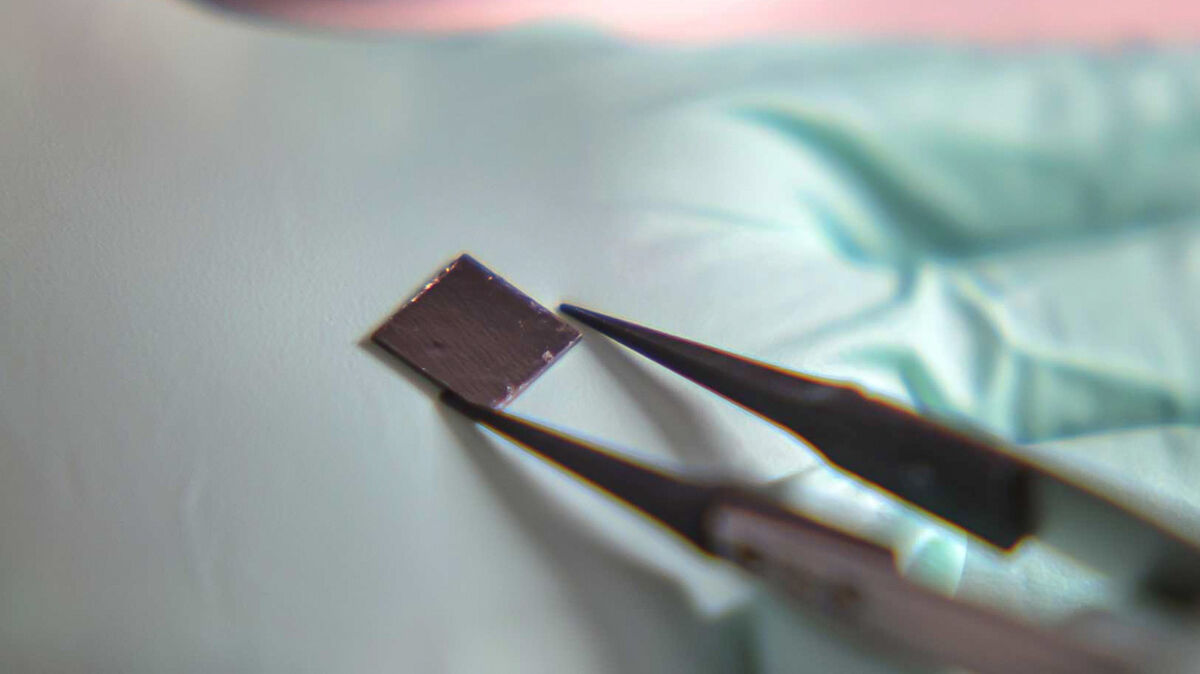
Ping Wang, a postdoctoral researcher in electrical engineering and computer science, checks a monolayer hBN-graphene sample grown by an ultrahigh temperature MBE system.
In a discovery that could speed research into next-generation electronics and light-emitting diode devices, a University of Michigan research team has developed the first reliable, scalable method for growing single layers of hexagonal boron nitride (hBN) on graphene.
Known as molecular-beam epitaxy – a process widely used in the manufacture of semiconductor devices, including transistors, and considered one of the fundamental tools for the development of nanotechnologies. This method of producing large sheets of high-quality hexagonal boron nitride is detailed fully in a study published in "Advanced Materials."
The ability to grow 2D hexagonal boron nitride on graphene opens the doors for numerous technological advances.
"Graphene-hBN structures have been found to power LEDs that generate deep-UV light, which is impossible in today's LEDs," said Zetian Mi, professor of electrical engineering and computer science at the University of Michigan and a corresponding author of the study.
Deep-ultraviolet LEDs – an LED that can emit light in the wavelength range called "UV-C" between 100 to 280 nanometers – are currently becoming particularly popular due to the capability of replacing mercury lamps, which have been the main source for UV light application equipment.
"The technology used to generate deep-UV light today is mercury-xenon lamps, which are hot, bulky, inefficient and contain toxic materials," said Mi. "If we can generate that light with LEDs, we could see an efficiency revolution in UV devices similar to what we saw when LED light bulbs replaced incandescents."
If such an innovation comes to market, such as in your nearest hardware store, a sterilization light could become commonplace and provide another source of protection against viruses and bacteria.
Deep-UV LEDs have a superior advantage compared to mercury lamps, such as their smaller size, higher efficiency, and zero warm-up time. For these reasons, as a general view in the UV light field, mercury lamps are soon to be replaced by deep-UV LEDs, although the issue of scalability had been preventing it from becoming largely adopted.
Hexagonal boron nitride is the world's thinnest insulator, while graphene is the thinnest of a class of materials called semimetals or metalloids, which has highly malleable electrical properties and are becoming more and more important for its role in computers and other electronics.
Bonding hBN and graphene together in smooth, single-atom-thick layers has led researchers to discover that it presents a veritable treasure trove of exotic properties. In addition to deep-UV LEDs, graphene-hBN structures could enable quantum computing devices, smaller and more efficient electronics and optoelectronics and a variety of other applications.
"Researchers have known about the properties of hBN for years, but in the past, the only way to get thin sheets needed for research was to physically exfoliate them from a larger boron nitride crystal, which is labor-intensive and only yields tiny flakes of the material," Mi said. "Our process can grow atomic-scale-thin sheets of essentially any size, which opens a lot of exciting new research possibilities."
While researchers have tried in the past to synthesize thin layers of hBN using methods like sputtering – much like the name, it uses a process of bombarding a solid target of the desired film material with energetic particles – and chemical vapor deposition – coating the desired film material in a reagent to chemically produce nanoscale films – they struggled to get the even, precisely ordered layers of atoms that are needed to bond correctly with the graphene layer.
"To get a useful product, you need consistent, ordered rows of hBN atoms that align with the graphene underneath, and previous efforts weren't able to achieve that," said Ping Wang, a postdoctoral researcher in electrical engineering and computer science. "Some of the hBN went down neatly, but many areas were disordered and randomly aligned."
The team, made up of electrical engineering and computer science, materials science and engineering, and physics researchers, discovered that neat rows of hBN atoms are more stable at high temperature than the undesirable jagged formations. Armed with that knowledge, Wang began experimenting with molecular-beam epitaxy, an industrial process that amounts to spraying individual atoms onto a substrate.
Using a terraced graphene substrate-essentially an atomic-scale staircase-and heating it to around 1,600 degrees Celsius (2,900 degrees Fahrenheit) before spraying on individual boron and active nitrogen atoms, Wang and team discovered results that far exceeded their expectations.
Neatly formed and ordered seams of hBN on the graphene's terraced edges, which could then expand into wide ribbons of material.
"Experimenting with large amounts of pristine hBN was a distant dream for many years, but this discovery changes that," added Mi. "This is a big step toward the commercialization of 2D quantum structures."


Reader Comments(0)